High-Rise Chips Avoid Conventional IC Limitations
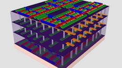
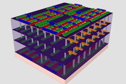
An engineering team at Stanford University has devised a way to improve computer chips by making them taller. According to the team, current chips suffer from “jammed wires" when the logic and memory components become overtaxed. Their solution--adding layers of logic atop memory and using electronic nanoscale “elevators” to move data between layers--eliminates bottlenecks created by wires and thereby moves data faster using less electricity.
It took the team three breakthroughs to be able to build a four-story prototype of their high-rise chip. The first was efficiently building nanoscale carbon-nanotube transistors (CNTs) that could be more completely sealed than current conventional transistors--which leak electrons, creating heat and wasting electricity. Until now, CNTs could not be grown together tightly. To get around this limitation, Stanford engineers grew CNTs on a quartz wafer and then used a metal film that acts like adhesive tape to lift them off the quartz and transfer them to a silicon wafer. After 12 more similar transfers, they had assembled one of the densest array of CNTs ever made, then used it as the foundation of their high-rise chip. It’s notable that the team could do this with lab equipment rather than the sophisticated gear used in commercial fabrication plants. Moreover, they showed this technique could build more than one layer of logic CNTs.
The Stanford team also came up with a method of building a new type of memory directly on top of the CNT layer. The memory is a metal-oxide-metal sandwich of titanium nitride, hafnium oxide, and platinum--there is no silicon. This sandwich resists current flow in one direction and allows it in the opposite direction. The change from resistive to conductive states lets this new memory --a resistive random access memory or RRAM--create digital zeros and ones. The new memory uses less electricity than conventional silicon memory and can be built at lower temperatures, so it is compatible with the high-rise manufacturing processes and materials.
The final breakthrough was drilling thousands of interconnections (nanoscale signal elevators) through the memory layers to the layers of CNTs below them. All those interconnects eliminate the traffic jams of signals common on conventional circuit cards. There is no comparable way to add interconnections between silicon-based memory and logic on conventional chips built as high-rises. That’s because it takes temperatures as high as 1,000°C to create silicon memory, and that would melt any logic components below.

