NIST Scientists Create Single-Atom Transistor
Transistors consisting only of several-atom clusters or even single atoms could become the building blocks of a new generation of computers with unparalleled memory and processing power. But first researchers need to develop a way to mass-produce tiny on-off switches.
Fortunately, researchers at the National Institute of Standards and Technology (NIST) together with colleagues at the University of Maryland have developed a step-by-step methods for making atomic-scaled transistors. Using the instructions, this group has become only the second in the world to construct a single-atom transistor and the first to fabricate a series of single-electron transistors with atomic-scale control over the devices’ geometry.
The scientists showed that the new electronic components can precisely adjust the speed at which individual electrons flow through a physical gap or electrical barrier in their transistor, even though classical physics forbids electrons from doing so because they lack enough energy. The electrons seemingly are getting away with quantum tunneling which only becomes possible when gaps are extremely small, such as in the miniature transistors.
Precise control over quantum tunneling is key because it lets the transistors become “entangled,” or interlinked, in a way only possible through quantum mechanics and opens new possibilities for creating quantum bits (qubits) that could be used in quantum computing.
To fabricate single-atom and few-atom transistors, the team covered a silicon chip with a layer of hydrogen atoms, which readily bind to silicon. The fine tip of a scanning tunneling microscope physically removes hydrogen atoms at selected sites. The remaining hydrogen acts as a barrier so that when the team directs phosphine gas (PH3) at the silicon surface, individual PH3 molecules attach only where the hydrogen has been removed. The researchers then heated the silicon surface. Heat ejected hydrogen atoms from the PH3 embed the phosphorus atom left behind into the surface. With additional processing, bound phosphorous atoms create the foundation of a series of highly stable single, or few-atom devices that can serve as qubits.
This animation shows the step-by-step recipe designed by NIST scientists and their colleagues to produce these atomic-scale devices. (Credit: S. Kelley/NIST)
To realize the full potential of their tiny transistors, researchers must find a way to make many copies of them.
Two of the steps in the method devised by the NIST teams—sealing the phosphorus atoms with protective layers of silicon and then making electrical contact with the embedded atoms—appear to have been essential to reliably fabricate many copies of atomically precise devices, said NIST researcher Richard Silver.
In the past, researchers have typically applied heat as silicon layers are grown to remove defects and ensure the silicon has the pure crystalline structure needed for single-atom devices with conventional silicon-chip components. But the NIST scientists found that such heating dislodges the bound phosphorus atoms and could disrupt the device’s final structure. Instead, the team deposited the first several silicon layers at room temperature, letting the phosphorus atoms stay in place. The team then applied heat as more layers were deposited.
Having even a single atom out of place can alter the conductivity and other properties of electrical components that feature single or small clusters of atoms.
The team also developed a new way of making electrical contact with the buried atoms so that will operate as part of a circuit. The NIST scientists gently heated a layer of palladium metal applied to specific regions on the silicon surface directly above certain components of the silicon-embedded transistor. The heated palladium reacts with the silicon to form an electrically conducting alloy called palladium silicide, which naturally penetrates the silicon and makes contact with the phosphorus atoms. This contact method has a nearly 100% success rate.
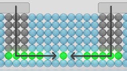
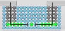
In related work, another research team recently showed it could precisely control the rate at which individual electrons tunnel through atomically precise tunnel barriers in single-electron transistors. This team also fabricated a series of single-electron transistors identical in every way except for the size of the tunneling gap. Measurements of current flow indicated that by increasing or decreasing the gap between transistor components by less than a nanometer, the team could precisely control the flow of a single electron through the transistor.
About the Author
Voice Your Opinion!
To join the conversation, and become an exclusive member of Machine Design, create an account today!

Leaders relevant to this article: