NIST Builds Testbed to Explore 3D Printing of Metal Parts
3D printing metal objects, also known as additive manufacturing (AM), is a booming industry, with the market for products and services worth more than an estimated $2.3 billion in 2015—a nearly five-fold growth since 2010. But the technology is still relatively new, and maintaining quality control can be challenging and time-consuming. Two products made in the same way on the same machine don’t necessarily come out with the same dimensions, says NIST’s Brandon Lane. And tiny pores can appear in layers, reducing the part’s strength properties. Residual stresses can build up as the layers cool, creating cracks between layers and warping the piece. The stress can be so high, in fact, it can warp a 1-inch-thick piece of steel by 0.04 inches.
To give engineers and manufacturers more control and predictability over 3D-printing metal parts, NIST researchers will build a testbed printer that will let them explore the process and develop ways to give users more control over their own 3D printing processes.
It will also let them answer critical questions such as: How hot does the melting metal get in each layer? How do you lower the stresses that cause cracking and warping? And what sensors would you need to provide better data on about what’s happening inside the printing machine?
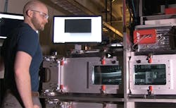
The testbed, more formally known as the Additive Manufacturing Metrology Testbed (AMMT), is a custom-made 3D printer that will let NIST researchers study the process in depth and produce tools users need to monitor the process in real time.
“In the additive manufacturing realm, there was already a push in industry to start putting sensors and monitors on their AM machines,” says Lane. “So we wanted to have those capabilities and to have a platform on which we could test new ideas for sensors.”
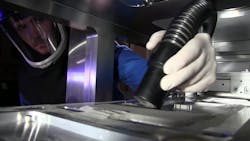
The AMMT is about the size of a small car and uses laser powder-bed fusion, a common technique in commercial AM printers. A mechanical arm applies a thin, even layer of metal powder to the surface of a flat metal plate. Then a high-power laser beam moves across the surface of this dusting of metal in the pattern needed for the piece being manufactured. The laser melts the powder, which briefly liquifies before cooling into a solid. When the laser is finished, a new layer of powder is applied, and the process repeats.
The AMMT is about the size of a small car and uses laser powder-bed fusion, a common technique in commercial AM printers.
Currently, the machine can use three different metals common to commercial AM: stainless steel, cobalt chrome, and a nickel alloy.
Unlike commercial systems, which use proprietary software, the AMMT lets researchers completely control the process. “Commercial printers are a little bit like a black box,” Lane says. “Users can dial in a certain laser power and velocity, but they really don’t control every single microsecond of the process. With our system, we control the speed and power of the laser at 100 kilohertz—that’s every 10 microseconds.”
Many AM process problems occur during melting, so the NIST team needed to find a way to precisely monitor the temperature of what they call the “melt pool,” the pool of molten metal liquid created while the laser heats up the powder. In this case, the team decided that best way to gauge its temperature is to measure properties of the light coming off of it. Materials turn different colors depending on how hot they are.
For now, the AMMT is set up to measure brightness, which researchers hope may be enough for many AM users. “They may only want relative measurements of the melt pool fluctuations,” Lane says. But the ultimate goal is to turn the relative measurements into absolute measurements, to use brightness and other properties as a way to gauge the melt pool’s actual temperature. To do this, the team will need to characterize the system and ensure the light intensity sensors are well-calibrated with standards.
“Eventually we’ll want to get to a full temperature map of the surface over a wide range of light wavelengths,” Lane says. The range will stretch from visible blue light at about 400 nm to mid-infrared (IR) light at 10 microns, which has wavelengths that are too long for the human eye to see.
Currently, the team uses a camera with a custom-designed achromatic lens to measure the pool’s brightness over some of the wavelengths they will eventually need, from reddish to near-IR light, at about 850 nm. “But at the higher temperatures, it’s bluer light, the shorter-wavelength visible light, that matters,” says researcher Steve Grantham. “So we’ll actually have some different way to measure that.”
He is referring to a device they are calling the Temperature and Emittance of Melts, Powders, and Solids (TEMPS). Emittance is a value that takes into account the ability of a substance to emit light at a particular temperature compared to how a black body would emit light. Knowing the emittance of the melt pool would help researchers understand how the melted metal was absorbing light and therefore help them calculate the melt pool’s temperature.
TEMPS will use a hemispheric reflectometer to collect data about the light reflecting off of the melt pool. The reflectometer will, in turn, let them map the emittance of the melt pool as well as its changing temperatures over time. And TEMPS will also include spectrographs, permitting measurement of the full visible and IR spectrum out to wavelengths of 10 microns.
A device like TEMPS would also be helpful for studying solid materials that experience extreme heat, such as the wingtips of supersonic aircraft.

