Thin Films Developed that Emit Single Photons at Specified Locations
A team of scientists at Los Alamos National Laboratory took another step closer to light-based quantum computing, cybersecurity, and other technologies when they demonstrated a way to create thin films that can control the emission of single photons.
“Efficiently controlling thin-film materials so they emit single photons at precise locations, what’s known as deterministic quantum emissions, paves the way for usable quantum materials,” says Michael Pettes, an LANL materials scientist.
The scalability of these two-dimensional, tungsten/selenium thin films helps makes them useful in quantum technologies. Single-photon generation is a requirement for all-optical quantum computing and some cybersecurity measures on communications.
The team took advantage of the strain at highly localized and well-separated emission sites, or tips, in a tungsten/selenium film. The team synthesized the film through chemical vapor deposition using a multi-step, diffusion-mediated gas source.
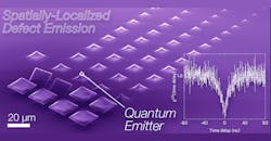
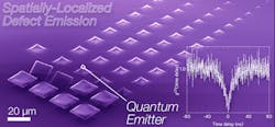
A new way to emit a single photon on command at specific locations in 2D materials may offer a new path to all-optical quantum computers and other quantum technologies. This image shows a false-color scanning electron micrograph of the array used to create single-photon sources in epitaxial tungsten diselenide. Inset shows the Hanbury-Brown Twiss interferometry measurement proving quantum emission.
Because the material is thin, it conforms to the radius of the tips and the material bends towards the substrate by more than a few percent, like someone lying on a bed of nails. The resulting strain is enough to change the electronic structure, but only at the tips. The affected area emits light of a different color and nature than light from the rest of the film.
“Although more research is needed to understand the role of mechanical deformation in creating these quantum emission sites, we may find a way to control quantum optical properties by using strain,” Pettes says. “These single-photon sources form the basis for photonics-based, all-optical quantum computing.”
Engineering quantum emissions in 2D materials is still in its early stage, the scientist notes. Earlier projects observed single photons originating from defects in these materials, suggesting that non-uniform strain fields might govern the effect. However, the mechanism responsible for this emergent phenomenon remains unclear and is the focus of ongoing work.


