CMOS (complementary metal-oxide-semiconductor) technology can be found in most all modern electronic devices—microcontrollers, microprocessors, and static RAM in both digital and analog form. We use CMOS for building those integrated circuits (ICs), but they haven’t changed much in terms of the semiconductor material they reside on (traditionally silicon). This limits CMOS’s data-processing speed, although it still maintains high noise immunity and low-static power consumption.
CMOS chip with integrated optical processing glass. (Credit: CUDOS)
To get around this issue and give CMOS a speed boost, scientists from Sidney’s ARC Centre of Excellence for Ultrahigh bandwidth Devices for Optical Systems (CUDOS), the Australian National University (ANU), and RMIT University developed a hybrid type of CMOS. It merges silicon with high-speed chalcogenide glass, providing an advanced alternative to conventional ICs.
Chalcogenide glass is a glass containing one or more chalcogens (sulfur, selenium and tellurium, but excluding oxygen). Such glasses are covalently bonded materials and may be classified as covalent network solids. The glass is often used for high-speed telecommunications, and can be found in a lot of today’s technology, including rewritable CDs/DVDs, lasers, planar optics, and PC-RAM. Integration of that glass into CMOS circuitry has supercharged the technology, resulting in processing speeds 100X faster over current CMOS standards. It also allows multiple functions to be integrated into those chips using both active and passive components—including microwave detectors and modulators.
How’d They Do That?
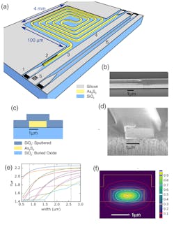
As2S3 silicon hybrid circuit. (a) Schematic of the hybrid circuit with a number of components indicated: 1. Silicon grating couplers with tapers to 450 nm×220 nm nanowires; 2. Silicon nanowire taper region with As2S3 overlay waveguide; 3. As2S3 waveguide lead into the hybrid structure; 4. Spiral waveguide formed out of As2S3; 5. Alignment markers formed in the silicon layer for patterning the As2S3 structures; 6. Reference silicon structures existing on the same chip. (b) SEM image of the end of the silicon taper before cladding deposition. (c) Schematic cross section of waveguide in chalcogenide-only region. (d) SEM image of chalcogenide region cross section with silica cladding. (e) Calculated effective indices for ten waveguide modes with increasing waveguide width. Waveguide widths used throughout the work, 1.9 μm in the spiral, 2.6 μm in the resonator, and 0.85 μm in the coupler, are indicated with dashed vertical lines. (f) Optical mode simulation of fundamental TE mode of 1.9 μm wide As2S3 waveguide. (Credit: CUDOS)
The recently published paper “Compact Brillouin devices through hybrid integration on silicon,” describes the manufacturing process of building the new hybrid circuit, outlining it with the graphic shown above. The process has a lengthy description, but the short version begins by using a silicon base section, which is then coupled with an active chalcogenide-glass deposition that has a nanowire waveguide sandwiched in between both materials.
The scientists describe it this way, “The fabrication of these devices uses silicon wafers from a semiconductor foundry in Belgium, a dedicated facility in ANU’s Laser Physics Centre for the glass deposition, lithography in the RMIT University’s School of Engineering, and are then characterized and tested in the University of Sydney’s AINST.”
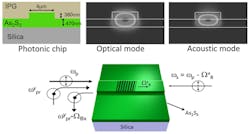
To highlight the potential of their new CMOS technology, the scientists demonstrated a novel laser, based on light/sound interaction, for the first time in an optical IC. This is also known as Brillouin scattering—the interaction of light and material waves within a medium, which is mediated by the refractive index dependence on the material properties of the medium; in this case, chalcogenide glass.
SBS Brillouin scattering on new CMOS technology. (Credit: CUDOS)
Their nanoscale optical phononic circuit makes use of nonlinear optical effects for more efficient interaction between phonons (sound) and photonics (light), giving that circuit a speed boost in processing information. “We integrated a novel nonlinear glass into an industrially scalable CMOS compatible platform. We maintained the key advantages of both the silicon and the glass, and made a functional and efficient ultra-compact optical circuit,” said CUDOS lead photonics nanofabrication manager, Dr. Alvaro Casas Bedoya (cited here).
According to the scientists, their new CMOS technology will one day allow industry manufacturers to miniaturize photonic functionalities from devices the size of laptops to those the size of smartphones and smaller, ultimately leading to deployment in real-world applications in the near future. To put it another way, the newly developed technology will go on to usher in the creation of tiny, optical circuits that can be manufactured in mass, which will no doubt become an industry standard in the next generation of mobile devices.
Some other possibilities for applications could include high-resolution, on-chip RF signal processors, advanced integrated microwave signal processing, and chip-based photonic Brillouin filters, among a host of others. One thing is for certain, traditional CMOS was developed by Frank Wanlass back in 1963, and we’re still using that technology today. So, It should be interesting to see what applications will integrate this new CMOS technology and what advances will spring forth with this latest development, which is on track to go beyond traditional RF systems.
About the Author
Cabe Atwell
Engineer, Machinist, Maker, Writer. A graduate Electrical Engineer actively plying his expertise in the industry and at his company, Gunhead. When not designing/building, he creates a steady torrent of projects and content in the media world. Many of his projects and articles are online at element14 & SolidSmack, industry-focused work at EETimes & EDN, and offbeat articles at Make Magazine. Currently, you can find him hosting webinars and contributing to Penton’s Electronic Design and Machine Design.


