New Materials Push the Embedded Tech Envelope

This file type includes high-resolution graphics and schematics when applicable.
Researchers have been finding new ways to embed sensors and other value-added devices into what some refer to as “smart materials.” While the definition can be debated, material properties and sensors are working hand-in-hand, opening doors to new applications that could change how engineers test and design parts.
“Engineers have been embedding sensors into materials for over 40 years,” notes Richard Claus, founder of NanoSonic. “I worked on some of this research in the 1970s with NASA, and the field has grown more popular and interesting ever since. It allows for creativity and out-of-the-box thinking, but it also means new challenges.”
For example, stress concentrations are a concern when embedding sensors into materials. Any inclusion can limit a product’s lifecycle or inhibit testing. Designing with new composite material was one way to solve this challenge. Engineers layered composites strategically around inclusions to redirect stresses around any electronics. Many of the electronics used are for testing in order to see stresses on materials during operation. This data can help calculate failure initiation loads.
“However, sensors can only collect data from the point at which contact is made,” says Michael Heflin, CEO for Sensuron. “This is limiting and makes it possible for engineers to design beyond their ability to test.” Using Von Mises criterion and, more recently, computer aided drafting with finite-element-analysis (FEA) software, engineers can predict stresses and strains between sensor contact points.
Although FEA offers accurate calculations on a wide array of materials properties with simulations, some applications require more data. Aerospace engineers, for example, rigorously test designs and materials. In one case, Boeing tested the wing box for the 787 using over 1,700 strain gages, which are still connected and wired manually (the wing box connects the wing to the fuselage and supports other subsystems such as the landing gear). Testing for the wing box required hooking up over 3,400 wires, which increased time spent, weight, and cost.
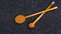
However, engineers have found new materials that could offer data from any point along a wing. It requires one wire that’s about the diameter of a human hair. By using a laser in the process of drawing out a fiber-optic cable, it makes a Bragg grating in the fiber that’s able to reflect light. These gratings can be put anywhere along the length of the fiber-optic cable.
“Fiber Bragg grating is able to acquire so much data at high speeds you would need a whole new testing platform in order to be able to process it all,” says Heflin. “Allen Parker is a systems engineer and he developed algorithms that made this possible. This platform is changing how we think about testing and design.”
Fiber Bragg Grating
NASA was researching fiber Bragg gratings (FBG) decades ago. “Traditional testing gages were not providing enough data. There are only so many strain gages you can affix to a part.,” says Heflin. “After a lot of research into better testing practices, scientists could use Bragg technology to measure stress at 1,400 points along the distance of a single fiber. It not only saved weight and time, but provided higher fidelity.”
Limiting factors affect the operating temperature and strain range of fiber-optic sensors. “It is the fiber that typically limits these ranges,” says Alex Tongue, applications engineer for Sensuron. “For example, different types of coatings can be used on a fiber-optic sensor to monitor different temperature ranges. Fiber sensors can have operational ranges of –422° to 1292°F, depending on the coating and type of fiber. Individual applications typically do not require this range, so most sensors fall somewhere in the middle. Sensuron usually uses fibers that operate from –422° to 599°F.”
A common coating that covers a wide temperature range is Ormocer, an organic modified ceramic hybrid polymer. It’s possible to reach higher temperatures by coating the fiber-optic sensors with different types of metals.
FBG can detect strain from –18,000 to 18,000 µε (micro-strain). The range depends on the laser used and type of fiber. Some sensors set the strain range using software. With the use of software, it’s possible to alter the strain range.
Companies that make FBG equipment are working with universities to teach students how to use this technology, which has many potential applications. For example, aerospace engineers could use it to determine wing loading while also providing accurate fuel readings. Automotive designers can determine maintenance and operational lives of vehicles. Civil engineers could monitor infrastructure “health” with the sensors. Overall, by embedding these fibers into products, it can save the time, money, and, weight associated with traditional strain gages and other sensors.
Materials Become Sensors
As sensors shrink and consume less power, they become easier to integrate with materials. Two forces driving the demand for smart materials are the need for more information and simplicity. Engineers can make more informed design decisions with more data obtained from testing. Collecting data during operation allows for better maintenance and offers real-world data for design.
Researchers are also working on complexity. Using materials science to generate multifunctional structures helps simplify products. For example, in 2002, the Naval Research Laboratory was developing multifunctional aircraft structures. One idea was to use a lithium polymer to serve as a battery while having the shape and function of a plane’s wing, reducing complexity and weight.
“We made a conductive rubber that measures strain, load, deformation, and extension,” says NanoSonic's Claus. “In its fabric form, it can be incorporated into other fabrics and materials like an embedded sensor. It works well with stiffer matrixes, so when it is deformed, the lower modulus stretchable sensor goes along for the ride without affecting the material’s dynamics.”
Ionomers and nanotechnology lets new flexible materials also be conductive. “Manufacturing them is much more interesting than some of the traditional processes,” says Claus. “Our approach is not taking an ingot and machining it down into a part. Instead, we use self-assembly. Chemists design the molecules, so they essentially grow the way you want them to.”
Simply explained, NanoSonic creates a solid matrix out of metal nano blobs in rubber that lets electrons move more freely than in the original material. Electrons “hop” between these blobs. The electrical resistance changes by altering the distance between blobs. It takes little metal to make some of these materials conductive. In fact, just 0.007% in volume can lead to good conductivities.
However, there are still challenges that lay ahead. Engineers are looking for better ways to communicate with smart materials and the devices inside them. Conductive materials connected by wires would mean stiff or brittle solder joints on what could be a moving, flexible part. In addition, stretching a wire or material that is transporting data or power can alter electrical resistance and interrupt the electric field, which could hinder the electronics performance.
“Designers are looking at the factory workers and field engineers needed to keep equipment functioning. If new materials can generate information to communicate better with these workers, it can save companies time and money,” says Claus. “Imagine if we could have coatings or materials like human skin. Seeing a machine tan or bruise could indicate something is wrong.”
A factory worker might be able to see a problem and prevent unscheduled maintenance, reducing downtime. A big focus for some things in the Internet of Things is a reduction in complexity in order to decrease power, thus allowing remote sensing. Access to remote data has proven to diminish the need for working on location.
A Feel for Applications
Being able to mimic human skin would have more value than just bruises. The ability to feel provides valuable information about the environment in which we interact. Researchers believe if machines were able to feel, it could prove valuable for many markets. For example, automation lines need to be dynamic, handle multiple products, and change easily. Engineers have developed scanners and grippers to accommodate these demands. But researchers are still trying to mimic human touch that can provide data on how to identify, pick-up, and handle a myriad of objects.
For more than a decade, many techniques have processed data that make it possible for a machine to feel. By using sophisticated torque sensors, the U.S. Defense Advanced Research Projects Agency (DARPA) was able to sense the resistance in picking up or making contact with objects. Stanford University was able to collect pressure readings with what are essentially rubber micro-pyramids with conductive nano-carbon tubes. As the material is compressed, the nanotubes become closer, increasing the conductivity. The amount of electricity flowing to the processor would then indicate pressure. These techniques could tell how hard or soft a machine or robot was gripping objects.
Scientists used chemistry to increase the amount of sensing elements on these new materials. Georgia Tech’s Zhong Lin Wang grew thousands of small, hair-like, zinc-oxide piezoelectric nanowire transistors. This technique led to a 15-fold increase in sensor density and spatial resolution when compared to the previous technology.
Beyond growing better sensors, materials science has presented new flexible composites and polymers. These materials are able to connect devices or provide data. A new polymer called polydimethylsiloxane, or PDMS, is a flexible transparent silicone with embedded nanoribbons. The electricity generated when the material is deformed can be processed to present tactical feedback. PDMS can detect temperature and humidity while offering a flexible and stretchable matrix, allowing for more complex electronics work in or on the material.
PDMS is used in the bulk of research for some of the most advanced materials. In general, organic field effect transistors like PDMS are merging materials and sensors.
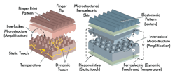
“Human touch is more complex than just collecting data. Our skin interacts with objects,” says Matt Borzage, the head of business development for SynTouch. “Our sense of touch has three main components. Skin feels an increased surface area as it wraps around an object. A fingerprint and nail can provide micro vibrations, and even the temperature of the skin interacts with the material being touched. Giving a robot features like a fingerprint or nails is not for aesthetics, but can increase sensitivity by a factor of 30. All of these features offer better data that can work with software to interpret hardness, surface roughness, temperature, thermal conductivity, and more. A person uses this information to determine how hard to grip, or what an object is. This is the same data we want a robot to offer to a production line or medical prosthetic.
“A challenge is when you find a blend of materials and sensors to mimic touch, and then realize the component isn’t robust enough for real-world applications,” continues Borzage. “By placing all electronics inside a rigid core and covering them with a compliant replaceable bladder, we came up with a sensor that is able to be more robust while providing sensitive human-like measurements.”
While this might sound like a convenience rather than a necessity, companies face having to justify the resources on an embedded device with the value added by simplifying systems, obtaining more data, or gaining better operation. The ability to "fell" an object to identify, handle, and process multiple objects dynamically has many manufacturers interested to see what will emerge from materials science.
About the Author
Jeff Kerns
Technology Editor
Voice Your Opinion!
To join the conversation, and become an exclusive member of Machine Design, create an account today!

Leaders relevant to this article: