Look Out, Silicon: Bio-Organic/Compatible Transistors are Coming on Strong
The search for biocompatible, implantable transistors to replace standard silicon-based devices as well as existing “organic” devices has attracted many potential entrants, each with apparent benefits and drawbacks. Now, a team comprised of researchers from the Columbia University School of Engineering, Columbia University Medical Center, and the Institute for Genomic Medicine has devised and tested what they maintain is the first biocompatible, ion-driven transistor that’s fast enough to enable real-time signal sensing and stimulation of brain signals.
Their ion-gated transistor (IGT—not to be confused with the IGBT) uses mobile ions within a conducting polymer channel to allow both volumetric capacitance via ionic interactions through the bulk of the channel, as well as shortened ionic-transit time. The transistor, which has relatively high transconductance and speed, can be used either as a single device or “microfabricated” to create the equivalent of integrated circuits.
In their detailed paper “Internal ion-gated organic electrochemical transistor: A building block for integrated bioelectronics” in the AAAS publication Science Advances, the researchers explain the theory, development, construction, test, and evaluation of devices. Also discussed is a soft, conformable interface with human skin that provided high-quality amplification of neural signals.
Assistant Professor and project leader Dion Khodagholy noted, “Our transistor’s channel is made out of fully biocompatible materials and can interact with both ions and electrons, making communication with neural signals of the body more efficient….[these devices] can be implanted in humans over long periods of time.”
The transistor is based on a channel using conducting polymers to enable ionic modulation. To speed the device, they modified the material to have its own mobile ions and also shortened the distance that ions needed to travel within the polymer structure. This increased the speed of the transistor by 10× compared to other ionic devices of the same size.
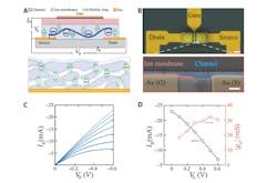
1. Structure and steady-state characteristics of IGT: Schematic illustration of IGT cross section and wiring diagram for device operation (top); d-sorbitol creates an ion reservoir for mobile ions (green) that can travel within the channel—the PEDOT-rich regions are shown in light blue and PSS lamellas in white (bottom) (A). Optical micrograph displaying the top view of an individual transistor [Scale bar, 20 µm] (B). Inset shows a cross-sectional scanning-electron-microscopy image acquired at a tilt angle of 30 deg. Ion membrane (light red), channel (light blue), and Au contacts for gate (G) and source (S; beige) are visible [Scale bar, 5 µm]. Output characteristics (ID − VD) of IGT device (L = 5 µm, W = 500 µm) for gate voltage (VG) varying from 0 V (top curve) to +0.6 V (bottom curve) with a step of +0.1 V; color intensity corresponds to VG amplitude (C). Transfer curve for VD = −0.6 V (black), and the corresponding transconductance (orange), |gmmax| = 32.30 ms. (D) (Source: Columbia University)
The channel of the IGT used a conducting polymer poly(3,4-ethylenedioxythiophene) polystyrene sulfonate (PEDOT:PSS) combined with d-sorbitol. (PEDOT:PSS is biocompatible, stable, and highly conductive, necessary for efficient ion-to-electron conversion; d-sorbitol is a biocompatible hydrophilic sugar alcohol that uptakes water molecules.) The transistor architecture was built by forming channels, each with independent ion reservoirs, between two gold-based source and drain electrodes (Fig. 1). To allow for independent gating of individual transistors, the gate electrode must have efficient ionic, but not electronic, conduction with the bulk of the channel.
Initial transconductance gm was 0.8 ms with a rise time of 31.7 µs. They also fabricated increasingly smaller IGTs and recorded a time constant of 2.6 µs with a 12- by 5-µm channel area, which corresponds to an effective bandwidth of 380 kHz. That’s several orders of magnitude faster than previously reported electrolyte-gated transistors, including those with smaller channel dimensions.
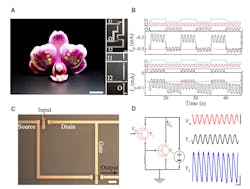
In a real-world application, they designed cascaded IGTs for multistage amplification and higher overall gain than a single transistor could provide (Fig. 2). IGT device T1 registered the input from its gate electrode and amplified it, and its output current was converted to voltage using a resistor and then connected to the gate of the second-stage transistor T2. They injected a 25-mV sine wave into the cascaded IGTs and observed a 4× increase in amplification versus the output of a single transistor.
2. IGT-based digital logic gates and cascaded amplifiers: IGT-based NAND and NOR gates conform to the surface of orchid petals (left) [Scale bar, 1 cm]; optical micrographs of NOR (top right) and NAND (bottom right) logic gates (A). Input (I1 and I2) and output (O) configuration is indicated [Scale bar, 100 µm]. Temporal response of the output (O) drain current of a NOR (top) and a NAND (bottom) logic gate (B). First input signal (I1, blue), second input signal (I2, red), and output signal (O, black) are shown at the top; dashed red lines mark the threshold of high and low logics. Optical micrograph displaying the top view of an IGT-based cascaded amplifier [Scale bar, 20 µm] (C). Circuit diagram of IGT-based cascaded amplifier and the corresponding input and output signals (D). Input voltage, Vin, (red) [Scale bar, 50 mV]; output signal from T1 (black) and final amplified output from T2 (blue) [Scale bars, 50 µA and 100 ms]. (Image sources: Columbia University; Photo credit: Jennifer Gelinas, Columbia University)
They further validated IGT performance by microfabricating devices that adhere conformally between human hairs on relevant electroencephalography (EEG) signals They were able to record human brain waves from the surface of the scalp, with a contact size five orders of magnitude less than existing devices. The entire device fit between hair follicles, substantially simplifying placement. Since the micro-EEG IGT device conforms to the scalp, no chemical adhesives were needed. As a result, the patient had no skin irritation from adhesives and was more comfortable overall.


