Image

Substrate-based thin-film circuits

July 23, 2014
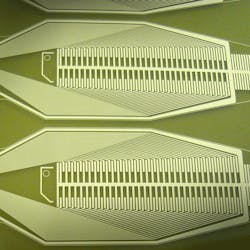
A new substrate-based additive fabrication technique eliminates the sloping caused during traditional chemical etching, which results in performance variations and yield issues.
A new substrate-based additive fabrication technique eliminates the sloping caused during traditional chemical etching, which results in performance variations and yield issues. The technique creates substrate-based, ultraminiaturized circuits with properties that include circuit lines and spaces as small as 10 μm, vias as small as 25 μm in diameter, plated through-holes to ground with “metal-backed” ceramics, and multilayer devices with up to six metal layers.

The process defines circuit lines by electroplating or sputtering metal traces onto either a rigid substrate in a single layer device or onto a polyimide layer in a multilayer device for extreme uniformity in geometries as well as the ability to deposit exactly the desired amount of metal in exactly the desired location.

Metrigraphics, 50 Concord St., Wilmington, MA 01887, (978) 658-6100

Sponsored Recommendations

June 27, 2025
Ensure workplace safety and compliance with our comprehensive Lockout/Tagout (LOTO) Safety Training course. Learn critical procedures to prevent serious injuries.
June 27, 2025
Join our expert webinar to discover essential safety control measures and best practices for engineering a truly safe and compliant industrial environment.
June 25, 2025
An innovative aircraft with electric drives combines the best of both worlds. The cross between drone and helicopter could mean significantly faster and more efficient air emergency...
June 25, 2025
Effective when other materials fail, ceramics are particularly suitable for applications requiring wear and chemical resistance, sliding characteristics or biocompatibility. Discover...

Voice your opinion!

To join the conversation, and become an exclusive member of Machine Design, create an account today!