Giant piezoelectric response enables nanopositioning
By integrating a complex, single-crystal material with “giant” piezoelectric properties onto silicon, University of Wisconsin-Madison researchers can fabricate low-voltage, near-nanoscale electromechanical devices. These devices could lead to improvements in high-resolution 3D imaging, signal processing, communications, energy harvesting, sensing, and actuators for nanopositioning devices.
Led by Dr. Chang-Beom Eom, the research team published its results in the Nov. 18 issue of Science. Piezoelectric materials use mechanical motion to generate an electrical signal. Conversely, piezoelectrics also can use an electrical signal to generate mechanical motion, such as the high-frequency acoustic waves used for ultrasound imaging. Eom studies the advanced piezoelectric material, lead magnesium niobate-lead titanate, or PMN-PT. Such materials exhibit a giant piezoelectric response that can deliver much greater mechanical displacement with the same amount of electric field as traditional piezoelectric materials. They also can act as both actuators and sensors. For example, they use electricity to deliver an ultrasound wave that penetrates far into the body and returns data capable of displaying a high-quality 3D image.
Currently, a major limitation of these advanced materials is that to incorporate them into very small-scale devices, researchers must start with a bulk material and grind, cut, and polish it to the desired size. This is an imprecise process not well suited for nanoelectromechanical systems (NEMS) or microelectromechanical systems (MEMS). Until now, the complexity of PMN-PT has thwarted efforts to develop simple, reproducable microscale fabrication techniques.
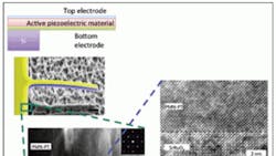
Applying microscale fabrication techniques such as those used in computer electronics, Eom's team has overcome that barrier. Because of potential chemical reactions among the components, researchers layered materials and carefully planned the locations of individual atoms.
The team calls devices fabricated from this giant piezoelectric material “hyper-active MEMS” for their potential to offer researchers a high level of active control. Using the material, the team also developed a process for fabricating piezoelectric MEMS.
Applied in signal processing, communications, medical imaging, and nanopositioning actuators, hyper-active MEMS devices could reduce power consumption and increase actuator speed and sensor sensitivity. Additionally, through a process called energy harvesting, hyper-active MEMS devices could convert energy from sources such as mechanical vibrations into electricity that powers other small devices, such as those used for wireless communication. For more information, visit engr.wisc.edu.
