Electro-Optical Ultrasound Detector Far Surpasses Piezoelectric Resolution, Sensitivity
This article appeared in Electronic Design and has been published here with permission.
What you'll learn:
- What is a SWED?
- How the research team's SWED design significantly improved imaging.
- Initial test results with the SWED design.
The standard two-dimensional array of piezoelectric sensors used for ultrasonic imaging suffers from the same tradeoff as many other sensing array technologies: If you reduce the element size to improve resolution, you also reduce sensitivity. Now, a German-based research team has devised an ultrasonic silicon-on-insulator (SOI) electro-optical detector that they maintain is not only the smallest by far, but also offers much greater resolution with superior sensitivity. Target applications include clinical diagnostics and basic biomedical research such as super-resolution imaging of cells and micro-vasculature in tissues.
The joint team from Helmholtz Zentrum München and the Technical University of Munich (TUM) says that their silicon waveguide-etalon detector (SWED) optical-resonator design offers a per-area sensitivity that’s four orders of magnitude (104) higher than the super-small alternative of an optical micro-ring resonators. On top of that, they say its eight orders of magnitude (108) higher than for standard piezoelectric detectors of the same size (which lose sensitivity proportional to the square of size reduction of their edge dimension).
The team also demonstrated an ultra-wide acoustic bandwidth reaching 230 MHz and performed imaging tests based on this ultrasound detector. The sensing area is about 200 times smaller than the ultrasound wavelength employed, which means that it can be used to visualize features smaller than one micrometer, thus leading to what’s called super-resolution imaging.
“The degree to which we were we able to miniaturize the new detector while retaining high sensitivity due to the use of silicon photonics was breathtaking,” says Prof. Vasilis Ntziachristos, who led the research team.
“This is the first time that a detector smaller than the size of a blood cell is used to detect ultrasound using the silicon photonics technology,” says Rami Shnaiderman, developer of SWED. “If a piezoelectric detector was miniaturized to the scale of SWED, it would be 100 million times less sensitive.”
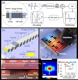
At the heart of the standard-process SOI device is a 220- × 500-nm SWED (Fig. 1). (An etalon—the “E” in SWED—is an interferometer with two parallel and partially silvered glass plates set a fixed distance apart; its multiple reflections yield interference spectra that can be used for wavelength tuning of lasers or as a narrowband filter.) Thus, instead of recording voltages from the piezoelectric crystals, the SWED monitors changes in light intensity propagating through the miniaturized photonic “circuits.”
By using an ultra-thin metallic layer for reflection rather than the usual Bragg grating, they were able to place the optical cavity in close proximity to the end facet of the waveguide. This allows for ultrasound detection through its cross-section, while the mirror’s thinness also minimizes attenuation of the ultrasonic waves that propagate from the reflective layer into the optical cavity.
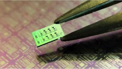
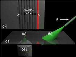
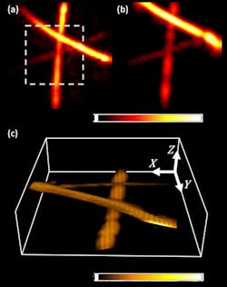
To verify performance, they manufactured eight SWEDs on a single SOI chip measuring 3 × 3 × 0.8 mm (Fig. 2) and used one test arrangement characterization and the other for imaging (Fig. 3). For the imaging, they performed tomography of a “phantom” triangular object made of three black polystyrene sutures with diameters of 10, 30, and 50 μm.
They illuminated this object with a pulsed 532-nm laser and 0.9-ns pulse width having an optical fluence (optical energy per unit area) of 2 mJ/cm2. They performed two raster scans using different scanning steps with the sample at a distance of 1.3 mm from the SWED.
The first scan was performed with a step size of 100 μm covering an area of 4 × 4 mm. The three sutures were clearly resolved, and the highest intensity was observed for the 50-µm suture lying on top of the others (Fig. 4). The second scan was performed with a step size of 50 μm over an area of 2 × 2 mm, for zoomed-in operation.
The work is described in detail in their paper “A submicrometre silicon-on-insulator resonator for ultrasound detection” published in Nature, along with Supplementary Information that provides quantitative analysis and modeling of the acoustic and optical path. The primary paper is behind a paywall, but fortunately an open copy is available here.
