New Fabrication Approach Yields High-Performance Flexible Electronics
What You’ll Learn:
- How a new approach to fabricating flexible circuits was devised.
- How this technique yields devices just a few atoms thick.
- Some performance specifications on the resultant flexible FETs.
Flextronics—meaning flexible electronics including the active and passive devices as well as their carrier (akin to a PCB)—is an attractive and hot area of interest, especially for wearables and even some IoT applications. However, developing such a carrier and components with superior flexibility and ruggedness, as well as sufficient electronic performance, has been a challenge.
Thus far, the primary engineering impediment has been the formation of these almost impossibly thin devices: It requires a process that’s far too heat-intensive for their flexible plastic substrates. These flexible materials would simply melt and decompose in the production process.
Steps to Making Flexible 100-nm Transistors
Now, researchers at Stanford University have devised a manufacturing approach that yields flexible, atomically thin transistors less than 100 nm in length—several times smaller than previously possible. Their solution is counterintuitive: They perform the process in a sequence of steps that starts with a rigid base substrate of silicon coated with glass (Fig. 1).
1. Transfer process for 2D monolayers with contacts: (a) Optical image of MoS2 and patterned metal covered by polyimide (PI) on SiO2/Si. (b) Schematic of the transfer process: the PI with embedded metal contacts and monolayer transition metal dichalcogenides (TMDs) are released from the rigid growth substrate. (c) Optical image of the flexible PI after transfer. Optical microscope images of (d), the SiO2/Si growth substrate after transfer (with the bare SiO2 surface where MoS2 had previously been covered by PI). (e) PI film with contacts and unpatterned MoS2 after transfer and (f) contacts with patterned MoS2 on SiO2/Si (top) and PI (bottom).
Next, they form an atomically thin film of the 2D semiconductor molybdenum disulfide (MoS2), one layer of atoms at a time, using chemical-vapor-deposition (CVD) techniques. Then it’s overlaid with small nano-patterned gold electrodes. While the resulting film is just three atoms thick, it still requires temperatures as high as 850°C to work. The traditional polyimide flexible substrate loses its shape at around 360°C and would be completely decomposed at those higher temperatures.
After first patterning and forming of these critical parts on rigid silicon and allowing them to cool, the Stanford researchers begin the process of applying it to the flexible material. Following a basic bath in deionized water, they peel back the entire device stack without damage and then fully transfer it to the flexible polyimide. Then a few additional fabrication steps complete the process.
“In the end, the entire structure is just 5 microns thick, including the flexible polyimide,” noted electrical engineering professor (and project leader) Eric Pop, commenting on this technique developed by Alwin Daus, a postdoctoral scholar in Pop’s lab.
What Are the Benefits?
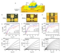
The resulting flexible field-effect transistors (FETs) are capable of several times higher performance than any produced before with such atomically thin semiconductors—here, “higher performance” means high current capacity along with low-power operation. They conducted extensive electrical-performance tests, including (but not limited to) the resultant graphs shown in Fig. 2. There are also additional parameter tables.
2. Flexible field-effect transistors (FETs) with transition metal dichalcogenides: (a) Schematic cross-section. Optical microscope images of FETs with (b) WSe2 (Type A); (c) MoSe2 (Type A) and (d) MoS2 (Type B), scale bars: 50 μm. Measured transfer and output characteristics of (e), (h), WSe2 (Type A), (f), (i), MoSe2 (Type A) and (g), (j), MoS2 (Type B). (The gate current, or IG, is often negligible, although for some devices it can limit the on/off ratio.)
“This downscaling has several benefits,” said Daus, who is “first author” of the paper. “You can fit more transistors in a given footprint, of course, but you can also have higher currents at lower voltage—high speed with less power consumption.” In addition, the gold metal contacts dissipate and spread the heat generated by the transistors while in use—heat that might otherwise jeopardize the flexible polyimide.
Of course, the process is far more complicated and subtle than indicated by this brief description. Full details are in their paper “High-performance flexible nanoscale transistors based on transition metal dichalcogenides” published in Nature Electronics (it’s behind a paywall, but an open copy is available here). There’s also a lengthy “Supplemental Information” posting that includes results of Raman spectroscopy, atomic force microscopy and photoluminescence testing as well as additional “conventional” electronic measurements.
Funding for this research was provided by the Swiss National Science Foundation’s Early Postdoc Mobility Fellowship, the Beijing Institute of Collaborative Innovation, the U.S. National Science Foundation and the Stanford SystemX Alliance.
This article appeared in Electronic Design.


